Semiconductor testing is a critical link running through the whole‑process of chip design, wafer manufacturing, packaging and testing. Its core purpose is to screen out semiconductor devices with performance failure, substandard parameters and defects, so as to guarantee the reliability, yield and stability of chips. It acts as the "quality gate‑keeper" of the semiconductor industry.
I. Core Testing Stages and Contents
·Wafer Manufacturing Stage Testing (Front‑end Testing): Tests are performed on unpackaged wafers to eliminate process defects in advance and reduce subsequent costs.
Wafer Surface Inspection: Optical inspection equipment (AOI) is adopted to check scratches, particle contamination, photolithography pattern defects and other flaws on the wafer surface.
Electrical‑parameter Testing: A probe station combined with a tester is used to carry out parameter tests on bare dies on the wafer, verifying whether voltage, current, frequency and other indicators meet design specifications.
Defect Analysis: Slicing and Scanning Electron Microscope (SEM) analysis are conducted on abnormal chips to locate problems arising from photolithography, etching, doping and other processes.
·Packaging‑testing Stage Testing (Back‑end Testing): Comprehensive tests implemented after chip packaging to simulate actual service environments.
Appearance and Dimension Inspection: Check appearance defects such as package flatness, lead deformation and cracks in packaging materials, and measure dimensional parameters including lead pitch and package thickness.
Electrical Testing: Including functional testing (verifying whether the logical functions of chips work normally), DC parameter testing (such as leakage current and threshold voltage) and AC parameter testing (such as propagation delay and frequency response).
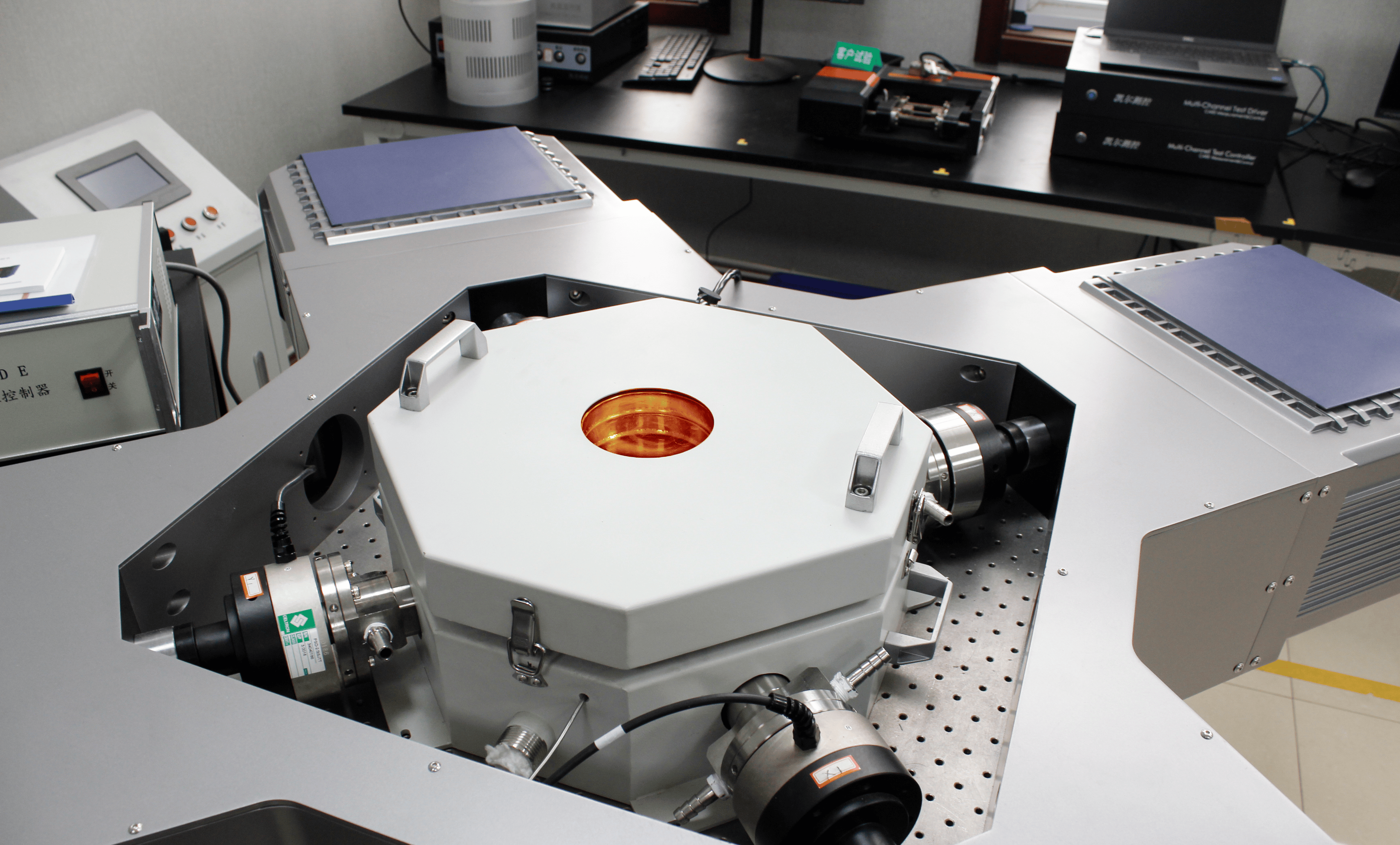
Reliability Testing: Simulate extreme operating environments to verify the long‑term stability of chips. Common items cover temperature‑humidity cycling test, damp‑heat aging test, salt‑spray test, Electro‑Static Discharge (ESD) test, Electromagnetic Compatibility (EMC) test, etc.
II. Common Testing Equipment
Front‑end Testing Equipment: Optical defect inspectors (AOI/ADI), Scanning Electron Microscopes (SEM), probe stations, wafer testers.
Back‑end Testing Equipment: Chip sorters, finished‑product testers, reliability‑test systems, appearance‑inspection devices.
III. Core Characteristics
Extremely High Precision Requirements: Nano‑scale subtle defects need to be detected, and the resolution of testing equipment shall reach sub‑micron or even nanometer level.
Full‑life‑cycle Coverage: Testing runs through every phase, from bare wafers to finished chips, from factory inspection to subsequent failure analysis.
High‑technical Barriers: Testing equipment integrates technologies from optics, electricity, materials science and other fields, belonging to high‑value‑added categories among semiconductor equipment.