Failure Analysis

Failure Analysis is a systematic technical activity that adopts scientific approaches to trace root causes, clarify mechanisms and propose improvement schemes for preventing similar problems when products, components or systems suffer functional anomalies, performance degradation, damage or even failure during expected operation. Its core purpose is to answer "Why the failure occurs, how it happens and how to avoid it", and it is widely applied in electronics, semiconductors, automotive and many other industries.

It delivers remarkable core values. First, to resolve immediate issues: rapidly locate root causes of faults such as chip burnout and component fracture, shorten troubleshooting time, and reduce losses caused by production suspension and customer complaints. Second, to prevent future risks: optimize design and improve manufacturing processes by analyzing failure mechanisms including material aging and design defects, so as to lower failure probability from the source. Third, to support quality control and R&D: simulate failure tests to verify reliability in the R&D phase and monitor batch quality during mass production. It serves as the key pillar for quality assurance and technical iteration.

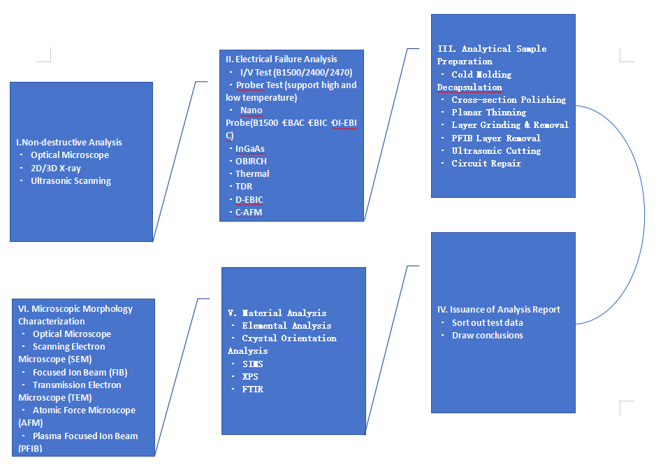
Take the electronics/semiconductor industry as an example. Firstly, confirm failure phenomena, record abnormal performance of products, and verify information such as service environment and production batches. Next, conduct non-destructive analysis for preliminary screening via visual inspection, electrical performance testing and other means. If further positioning is required, carry out destructive analysis including chip decapsulation and cross-section polishing. Afterwards, judge failure mechanisms combined with test data, and finally propose and track improvement plans.

It covers a wide range of application scenarios. In the semiconductor industry, analysis of chip failures constitutes a core technical link for relevant enterprises. In the automotive industry, troubleshooting failures of automotive electronics and mechanical components safeguards driving safety. In the medical device industry, identifying defects of diagnostic and implantable equipment matters to medical safety. In forensic appraisal, analysis of failed products provides technical evidence for liability confirmation.

Failure Analysis acts as a bridge connecting fault resolution and quality improvement. It is not only an "emergency tool" for enterprises to tackle unexpected problems, but also a "technical cornerstone" driving the industry toward higher reliability and safety.



Failure Analysis Classification

image.png

Non-Destructive Analysis

·SAT   ·2D X-Ray   ·3D X-Ray:ZEISS Xradia 620 Versa

3D X-Ray:

  1. Enable high-resolution imaging of large-size samples at a long working distance, with a maximum resolution of 0.5 μm;

  2. Voltage range: 30KV-160KV, maximum output power: 25W;

  3. Sample stage travel: 50mm*100mm*50mm.


Comprehensive Analysis

1. Failure Location


InGaAs

OBIRCH

Thermal

Power Limit

External connection available

25V/100μA, 10V/100mA

External connection available

Analysis Speed

Fast

Fast

Fast

Capture Characteristic

Photon

Resistance variation after laser heating

Thermal (Non-destructive optional)

Wavelength Range

900nm~1700nm

NA

3.7μm~5.2μm

Analysis Cases

MOSFET leakage, IC leakage (μA level)

IC short circuit, resistive leakage

IC leakage, short circuit, PCB short circuit, LU failure localization

Difficult-to-Analyze Defects

Metal shielding, resistive defects, non-photon-emitting defects

Metal shielding with poor heat absorption, interference from polycrystalline resistors or bias electric field

Low power consumption and low heat generation


2. Sample Preparation

·Polish: Perform targeted/non-targeted polishing; combined with Ion Milling to achieve clearer cross-section results.

·Decap: Gold wire, copper wire, palladium-coated copper wire, silver wire and various packages including ultra-small packages.

·Delayer: RIE adopts plasma gases such as O2, CF4, CHF3, SF6 to remove materials including Oxide, Nitride, Polyimide and Si. Physical polishing is combined for layer removal of advanced chips and BSI samples.


3. SEM Scanning Electron Microscope / Dual Beam FIB

HWD’s SEM fleet includes cold field and thermal field SEMs from multiple brands to support high-resolution observation. Equipped with EDS for surface composition analysis of samples. YAG detector delivers higher-quality images. Multiple DB FIB systems are available for nanoscale sample preparation. The combination of cold and thermal field equipment enables comprehensive data acquisition for customers.


4. FIB Circuit Modification

FIB Circuit Modification Equipment Thermo ScientificTM CENTRIOS

The circuit modification system supports circuit editing for aluminum-process, copper-process and gold-process samples.


5. Nanoprober NP8000

Specifications

Applications

100eV Probe Voltage

Effectively avoid charge accumulation, improve SEM resolution, and ensure no irradiation-induced electrical damage to state-of-the-art process devices.

DI-EBAC: EBAC function with applied voltage

Maximum beam current of 200nA enables hotspot capture at lower magnification to boost analysis efficiency. Upgraded DI-EBAC amplifier supports localization of short circuits below 10Ω and complete characterization of current loops.

EBAC

Locate critical failures in 3D interconnect structures with resistance as low as ~100Ω.

Pulsing IV Measurement

Detect high-resistance gate phenomena.

IV Measurement: 0.1fA/0.5V measurement resolution

Supports measurement with 8 probes.

High-Low Temperature Test

Reproduce high/low temperature failures within the range of -50℃~150℃.


FAQ
 
Our Advantages
Authoritative Qualifications

HWD | HuaWayDa is a comprehensive third-party service institution integrating inspection, testing, metrology, certification, training and enterprise technical services. It consists of Management Center, Marketing & Customer Service Center, Laboratory, Certification Center, Management Institute, Sustainable Development Center and Enterprise Service Center, and is committed to providing customers with professional, efficient and authoritative one-stop enterprise solutions.

HWD | HuaWayDa holds CNCA approval certificate, CMA qualification, measurement standard assessment certificate, CNAS accreditation and other relevant qualifications.

We strive to build long-term and mutually trustful partnerships with clients. We are not merely a service provider for your current projects, but also a reliable think tank and companion on your journey to pursue excellent management.

Choosing us means you are not only selecting a service, but also a long-term partner rooted in professionalism with your success as our mission. We promise to help you build a solid management foundation and sustainable competitive advantages with our professional capabilities.

Submit Your Requirements Now
Our expert team delivers premium solutions for you
Recommended Services
Related Downloads

Tel:021-6409 0330
         13917723034

Email:info@huawayda.com

© Copyright Huaweida Testing & Certification (Shanghai) Co., Ltd. All Rights Reserved ICP Filing/License No.: 16029900-1