Semiconductor Testing

Semiconductor testing is a critical link in the semiconductor industrial chain to ensure device performance, reliability and quality. A series of electrical, physical and environmental tests are conducted to verify whether chips comply with specification requirements throughout the full lifecycle from design to mass production. Its core objectives are to screen out non-conforming products, optimize production processes and reduce risks in downstream applications, and it is widely applied to semiconductor products such as integrated circuits (ICs), discrete devices and sensors.


Semiconductor testing runs through the entire process from design to shipment, and can be divided into the following four categories by stage:

1. Design Validation Test (DVT)

  • Purpose: Verify the correctness of design schemes, functional integrity and performance compliance before chip tape-out (mass production), so as to avoid mass production losses caused by design defects.

  • Test Contents:

    • Functional Test: Verify whether the chip realizes all designed functions (such as CPU instruction sets and GPU rendering functions);

    • Performance Test: Test whether key parameters (such as frequency, power consumption and latency) meet design specifications (e.g. "Main frequency ≥3.0GHz", "Standby power consumption ≤5mW");

    • Boundary Condition Test: Verify chip stability under extreme voltage and temperature (e.g. normal functions under minimum/maximum operating voltage).

  • Features: Small sample size (usually dozens of engineering samples), relying on manual or semi-automatic test platforms, long test cycles (several weeks to months).

2. Wafer Test (WT / CP - Chip Probe)

  • Purpose: Test each bare die on the wafer before wafer dicing to screen out defective chips and reduce subsequent packaging costs (avoid packaging defective dies).

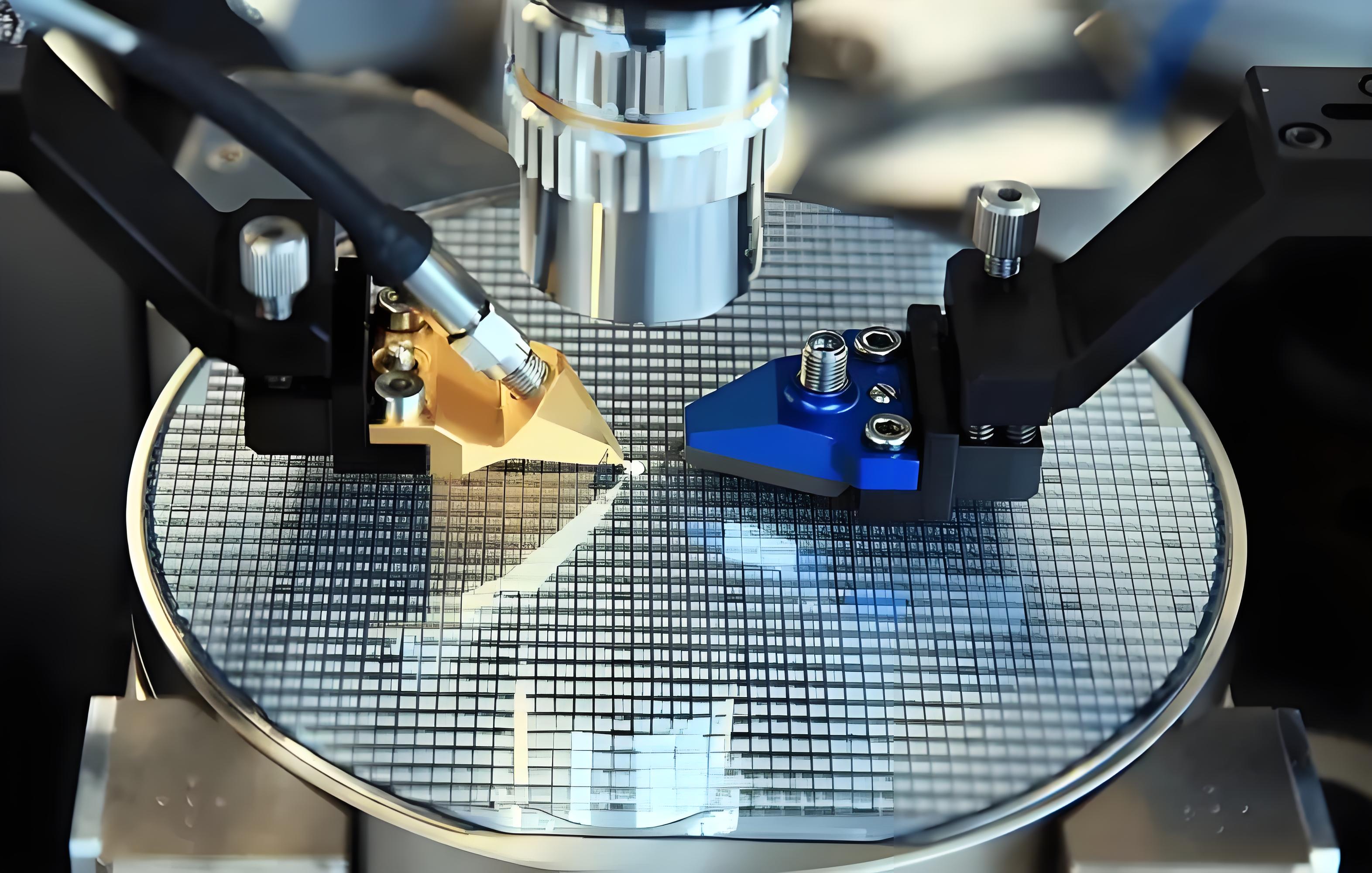
  • Test Scenario: The wafer is fixed on a prober. Probes make contact with the test pads of chips, and test equipment applies signals and collects responses.

  • Core Test Items:

    • DC Parameter Test: Such as leakage current (Iddq, quiescent power current), operating voltage (Vdd), pin continuity (to avoid short/open circuits);

    • Basic Functional Test: Verify normal core chip functions (e.g. read-write functions of memory chips);

    • Preliminary Performance Test: Basic indicators such as frequency and speed (e.g. "stable operation at 1GHz").

  • Features: Fast test speed (to match wafer mass production efficiency), coordinated operation of automatic probers and test equipment, moderate test coverage (only screen obviously defective dies).

3. Final Test (FT)

  • Purpose: Conduct comprehensive testing on finished chips after chip packaging (such as QFP, BGA and SiP packaging), to ensure no defects are introduced during packaging (e.g. broken leads, poor heat dissipation) and that performance meets shipment standards.

  • Test Scenario: Packaged chips are loaded via automatic equipment (such as a test handler), make contact with test sockets, and testing is completed by an Automatic Test Equipment (ATE).

  • Core Test Items:

    • Full Function Test: Cover all functional modules of the chip (such as CPU, GPU, ISP and interfaces of SoC);

    • AC Parameter Test: Test timing characteristics of high-frequency signals (such as Setup Time/Hold Time and signal transmission delay);

    • Power Consumption Test: Power consumption under different loads (e.g. full-load power consumption, dynamic power consumption);

    • Pin Integrity Test: Verify continuity of packaged pins (to avoid poor soldering or broken leads during packaging).

  • Features: High test coverage (nearly 100%), relying on high-speed ATE equipment, fast test speed (several chips can be tested per second), serving as the main testing stage in mass production.

4. Reliability Test (RT)

  • Purpose: Evaluate chip stability under long-term service or harsh environments, predict service life, and ensure compliance with reliability requirements of downstream applications (e.g. automotive electronics require "automotive-grade" reliability).

  • Test Standards: Follow standards such as JEDEC (Joint Electron Device Engineering Council) or AEC-Q (Automotive Electronics Council). Common test items include:

    • High Temperature Operating Life (HTOL): The chip operates continuously at high temperature (e.g. 125℃) and rated voltage for 1000-2000 hours to test performance degradation;

    • Temperature Cycling (TC): Hundreds of cycles between -55℃ and 125℃ to test the chip's resistance to thermal stress (prevent package cracking and solder joint detachment);

    • Electro-Static Discharge (ESD): Simulate human or machine discharge (e.g. HBM Human Body Model, MM Machine Model) to test the chip's resistance to electrostatic breakdown (e.g. HBM ≥2kV);

    • Moisture Sensitivity Level (MSL): Evaluate chip reliability in humid environments (avoid package cracking caused by water vapor expansion during soldering).

      Features: Small sample size (usually 1-5% of the batch), long test cycles (several weeks or even months), mandatory test items for "automotive-grade" and "industrial-grade" chips.


Core Test Items

1. Electrical Performance Test

Evaluate whether the electrical characteristics of the chip comply with design specifications, which is the most fundamental test item:


  • DC Parameters: Voltage (Vdd, Vss), Current (operating current, leakage current), Resistance (inter-pin resistance for short/open circuit judgment);

  • AC Parameters: Frequency (maximum operating frequency), Timing (signal setup/hold time), Propagation Delay (input-to-output response time);

  • Functional Parameters: Verify the implementation of all designed functions (e.g., instruction execution of CPU, analog-to-digital conversion accuracy of ADC).

2. Physical Defect Test

Detect physical defects generated during chip manufacturing (such as fabrication defects and packaging defects):


  • Optical Inspection: Use AOI (Automatic Optical Inspection) and AFM (Atomic Force Microscope) to observe lithography defects, scratches and contamination on wafer surfaces;

  • Acoustic Inspection: Detect internal voids and delamination inside packages via SAM (Scanning Acoustic Microscope) (e.g., solder voids between chip and substrate);

  • X-Ray Inspection: For complex packages such as BGA and SiP, X-ray is adopted to check cold solder joints and short circuits of solder bumps.

3. Environmental Adaptability Test

Simulate the performance of chips under various application environments:


  • Temperature Test: High & low temperature operating/storage test (e.g., -40℃~85℃ for industrial grade, -55℃~125℃ for automotive grade);

  • Vibration / Shock Test: Simulate mechanical stress during transportation or service (automotive electronics shall withstand vibration of 10–2000Hz);

  • Radiation Test: For aerospace and military chips, test radiation resistance (such as Total Ionizing Dose (TID), Single Event Upset (SEU)).


Scope of Application
  • Consumer Electronics (e.g., mobile phones, computers): Focus on performance indicators such as frequency and power consumption as well as basic reliability with low test costs. Faulty dies are screened out via FT test;

  • Automotive Electronics (e.g., automotive chips): Must comply with AEC-Q standards and undergo stringent reliability tests including 1000-hour HTOL and 1000-cycle temperature cycling, with full-item 100% testing required;

  • Industrial Control (e.g., PLCs, sensors): Require wide-temperature-range operation from -40℃ to 85℃ and EMC anti-electromagnetic interference tests with long reliability test cycles;

  • Aerospace & Military Products: Need to pass extreme environmental tests including radiation resistance and vacuum resistance, with nearly 100% test coverage and high testing costs.


FAQ
 
Our Advantages
Authoritative Qualifications

HWD | HuaWayDa is a comprehensive third-party service institution integrating inspection, testing, metrology, certification, training and enterprise technical services. It consists of Management Center, Marketing & Customer Service Center, Laboratory, Certification Center, Management Institute, Sustainable Development Center and Enterprise Service Center, and is committed to providing customers with professional, efficient and authoritative one-stop enterprise solutions.

HWD | HuaWayDa holds CNCA approval certificate, CMA qualification, measurement standard assessment certificate, CNAS accreditation and other relevant qualifications.

We strive to build long-term and mutually trustful partnerships with clients. We are not merely a service provider for your current projects, but also a reliable think tank and companion on your journey to pursue excellent management.

Choosing us means you are not only selecting a service, but also a long-term partner rooted in professionalism with your success as our mission. We promise to help you build a solid management foundation and sustainable competitive advantages with our professional capabilities.


Submit Your Requirements Now
Our expert team provides high-quality solutions for you
Related Downloads

Tel:021-6409 0330
         13917723034

Email:info@huawayda.com

© Copyright Huaweida Testing & Certification (Shanghai) Co., Ltd. All Rights Reserved ICP Filing/License No.: 16029900-1